4.1
UNDERSTANDING CATHODE RAY OSCILLOSCOPE

1. Metal consists a large number of electrons
2. At room temperature, the electrons are free to move but remain inside
the metal.
3. If the metal is heated at a high temperature, some of the free
electrons
may gain sufficient energy to escape from the
metal.
4. Thermionic emission is the process of
emission of electrons from
a heated metal’s surface.
5. Cathode rays tube.

6. Properties of cathode rays
a) Negatively charged particles called electrons.
b)Travel in straight lines and cast sharp shadows.
c)Travel at very high speed and have kinetic energy.
d) Can cause fluorescence. (A process where the kinetic energy of the
electrons is converted into
light energy)
e) Deflected by electric and magnetic fields.
7. Cathode rays can be used in
a) picture tube of a television
b) cathode ray oscilloscope (C.R.O)
c) visual display on a radar screen.
8. Maltese
cross cathode ray tube

a) 6.0 V power supply is switched on,
i) the filament is heated.
ii) the Maltese cross shadow is formed on the screen due to the light
from the filament
b) EHT power supply is switched on,
i) a high voltage is applied between the cathode and anode
ii) causing electrons to accelerate at high speeds
iii) these electrons are the cathode rays
iv) cathode rays travel in straight lines
c) The Maltese Cross blocked the cathode rays causing a shadow to form
on the screen.
d) The green screen formed around the shadow shows that the kinetic
energy of the electron is converted into light energy when the
electrons hit the fluorescent screen.
e) When a strong magnet is placed at the side of the Maltese Cross tube,
the shadow formed is moved and distorted. It shows that cathode rays
are
deflected by a magnetic field.
UNDERSTANDING CATHODE RAY OSCILLOSCOPE (C.R.O)

1. Components in a (C.R.O)
a)vacuum glass tube
b)an electron gun,
c)deflection system for deflecting the electron beam
d)fluorescent coated screen
2. Electron gun - produce a narrow beam of electrons
Component
|
Function
|
Filament
|
heat up the cathode.
|
Cathode
|
heated cathode emits electrons through the process of thermionic
emissions.
|
Control grid
|
control the number of electrons in the electron beams.
|
Focusing anode
|
focus the electrons into a beam and to attract electrons from the area
of the control grid.
|
Accelerating anode
|
accelerate the electron beam towards the screen.
|
3. Deflection
System - allows the electron beam to be deflected from its straight-line path when it leaves the electron gun.
Component
|
Function
|
Y-plates
|
move the electron beam vertically up and down
|
X-plates
|
move the electron beam across the
screen horizontally from left to right
|
4. Fluorescent
Screen - coated on the inside surface with some fluorescent
material such as phosphor or zinc sulfide.
Component
|
Function
|
Moving electrons
|
have kinetic energy and strikes the screen,
|
Fluorescent coating
|
converts the kinetic energy of the
electrons into light energy.
|
5. Application of
CRO
a) Measuring
potential difference
b) Measuring
short intervals
c) Displaying
wave forms
4.2 UNDERSTANDING SEMICONDUCTOR
DIODES
Semiconductors
1. are
metals whose conductivity lie between good conductors and insulators.
Conductor (Metals)
|
Good conductors of electricity
|
Very low resistance (generally)
|
Have free electrons that can move easily between
atoms
|
Insulators
|
Poor conductors of electricity.
|
Very high
resistance.
|
Have very few free electrons to
move about
|
Semiconductors
|
Conductivity
between conductor and insulator.
|
Resistance between conductors and insulator.
|
At 0 Kelvin
behaves as an insulator.
Temperature
increases
conductivity increase,
resistance will be lowered.
|
2. Pure
semiconductors
a) Tetravalent
elements
b) Each
atoms have 4 electrons in the outermost shell
c) Examples:
silicon, germanium and selenium

3. Doping
is a
process of adding a certain amount of specific impurities (dopants)
to a pure
semiconductor to increase its electrical conductivity.
4. Type of semiconductors
a)
n-type
b)
p-type

Aspect
|
n-type
Semiconductor
|
p-type
Semiconductor
|
Pure semiconductor
|
silicon
|
silicon
|
Dopants material
|
phosphorus, arsenic, antimony
|
boron, aluminium, gallium
|
Function of the
dopants material
|
produce an
abundance of electrons
|
create an abundance
of holes
|
Valens electrons of
the dopant material
|
pentavalent atoms
|
trivalent atoms
|
Majority charge carriers
|
free electrons
|
the holes
|
Minority charge carriers
|
the holes
|
free electrons
|
SEMICONDUCTOR DIODES

1.Diode
is
a) made
by joining a p-type and n-type semiconductors.
b) a
device that allows current to flow in one direction only
(blocks it in the opposite directions).
c) the
simplest semiconductor device.
2.pn junction is formed when a
n-type and p-type semiconductors are
joined together. The boundary between the
p-type and n- type regions
is called the junction.

3.Depletion layer is the neutral region around the junction which has no
charge carriers (left with neither holes nor free electrons). The conductivity
of electric is poor

4. Forward bias
a) p-type
is connected to the positive terminal of a battery.
b) n-type
is connected to the negative terminal of a battery.
c)The
diode conducts current because the holes from the p-type material
and the
electrons from the n-type material are able to cross over the junction.
Hence
the light bulb will light up.

5.Reversed bias
a)n-type
is connected to the positive terminal of the battery.
b) p-type
is connected to the negative terminal of the battery.
c) Reversed
polarity causes a very small current flows as both electrons
and holes are
pulled away from the junction.
d)
The depletion region widen and the
current will cease. Hence the bulb
does not light up.

6.Diodes as rectifiers
a) A rectifier is an
electrical device that converts alternating current to direct current.
b) Rectification is a
process to convert an alternating
current into a direct current
by
using a diode.
c) Two type of
rectification:
i) Half-wave rectification
ii) Full-wave
rectification
7. Rectification
a) A process where only half of every cycle
of an alternating current is made to
flow in one direction only.
b) No rectification

8. Half-wave rectification by
using one diode

a) A diode is connected in series with the resistor
b) Diode can only allow current to flow in one direction.
Current will only
flow in the first half-cycle when the diode in forward bias.
c) Current is blocked in the second half-cycle when the
diode is in reverse bias.
9. Full-wave rectification by using four diodes

a) In the first half, the current flows from A – P
– T – U – R – B
b) the second half, the current flows from B – Q –
T – U – S – A
10. The use of a capacitor in a
rectifier circuit

a) Capacitor is used to smooth out the output current and output voltage
b) When the current pass through the capacitor, the
capacitor is charged and
stores energy.
stores energy.
c) When there is no current pass through the capacitor, the
capacitor is discharged.
d) The energy from it is used to produce voltage across the resistor. As a result it produces a smooth dc output.
d) The energy from it is used to produce voltage across the resistor. As a result it produces a smooth dc output.
4.3 TRANSISTOR
1. A transistor has three leads connected to the emitter, E,
base, B and
collector, C
2. The emitter, E emits or sends charge carriers through the
thin base, B layer
to be collected by the collector, C

3. Two-type of transistor:
i) n-p-n transistor
ii ) p-n-p transistor
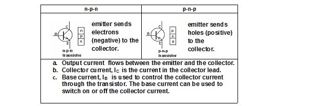

4. IB is too small compared to IC. [ IB <<<<<< IC]
i) IB unit
is μA
ii) IC unit
is mA
5.
Transistor
as a current amplifier
a) A small change in the
base current, results in a big change in the
collector current,

b) Base current is amplified by the transistor.
Hence M2 is brighter than M1
6. Transistor as an automatic
switch

a. Suitable resistor R1 and a variable resistor R2
is used .
b. Voltage at base
terminal can be adjusted to switch the transistor on or
off.
c.
If R2 increases, base voltage also increases
d.
When
the base voltage reaches certain minimum value, the base current
flows and switches the transistor on.
e.
Examples
of application of automatic switch are
i)
Light
control switch
ii)
Fire
alarm / Heat detector / Smoke detector


Light controlled switch

Examples:

a. Name terminal P, Q and R.
b. What is the function of Y
c. In order to light up the bulb, the potential difference
across EF must be
at least 4V.
i) What is the resistance of X when the bulb
lights up?
ii) What happen to the light bulb if X has
resistance of I KΩ?
d. What must be done to the circuit so that the bulb is
switched off in the bright light and on in the dark.
Answer:
a. P = base
Q =
collector
R =
emitter
b.
To limit the amount of current flowing into the base terminalc.

d. Replace
X with a light dependent resistor (LDR)
4.4 ANALYSING LOGIC GATES
1. Logic gate is a
circuit that has
a) one or more input signals, but
b) only one output signal.
c) act as switching circuits in
electronic systems
d) work using tiny transistors as
switches,
e) manufactured as integrated
circuit (IC), with each chip holding several gate
f) The input or inputs are on the left of the symbol.
g) The output is on the right
h) Each input and output can be either
2. Five logic gates:
- AND
- OR
- NOT
- NAND
- NOR
3. Symbol and Truth Table of the logic gates:

No comments:
Post a Comment